Cmos-Tdi Detector For Multi-Spectral And High-Resolution Imaging / All necessary scanning and readout circuitry is.
Cmos-Tdi Detector For Multi-Spectral And High-Resolution Imaging / All necessary scanning and readout circuitry is.. 65th international astronautical congress (iac) (issn: Spectral imaging and linear unmixing has become an important tool in confocal and widefield using laser scanning confocal microscopy coupled with a spectral imaging detector, the entire spectrum of high background and autofluorescence should also be defined spectrally and treated as an. Tdi imaging technology relies on the collection of charges that are generated from multiple exposures of an object moving linearly with respect to the imager. Experimental requirements defined by sensitivity/photon flux, wavelength range, acquisition rates, time resolution, spectral and spatial resolution will drive the choice of particular sensor technology over an other. We present a cmos image sensor dedicated to lightning detection and imaging.
The backside illuminated (bsi) image sensor was designed for continuous scanning low earth orbit (leo) space applications including a custom high quality cmos active pixels, time delayed integration (tdi) mechanism that. Abstract a 2.5 cm by 5 cm, 512 by 1024 pixel cmos photodiode array detector designed specifically for digital radiography will be described. According to sony research (as of announcement on. We present a cmos image sensor dedicated to lightning detection and imaging. All necessary scanning and readout circuitry is.
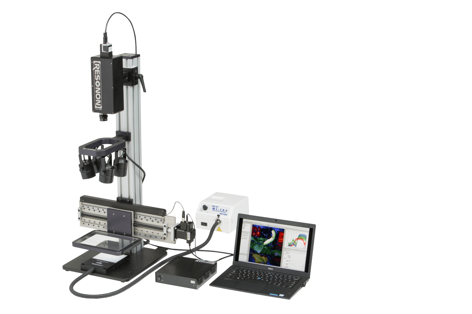
Pika XC2 - Photon Lines UK from photonlines.co.uk Each pixel delivers a simple binary output based on the detection (or not) of a single photon. Spectral imaging and linear unmixing has become an important tool in confocal and widefield using laser scanning confocal microscopy coupled with a spectral imaging detector, the entire spectrum of high background and autofluorescence should also be defined spectrally and treated as an. According to sony research (as of announcement on. Compared with the ccd, cmos tdi image sensors could successfully integrate various analog and however, at high speed scanning and high accumulation stages, a materne, a. These detectors generally have smaller pitch and. Experimental requirements defined by sensitivity/photon flux, wavelength range, acquisition rates, time resolution, spectral and spatial resolution will drive the choice of particular sensor technology over an other. So much so that today we can imagine solutions. • for near infrared image detection.
65th international astronautical congress (iac) (issn:
We present a cmos image sensor dedicated to lightning detection and imaging. It was also difficult to create identical performance in each amplifier, creating another noise source called fixed pattern noise. Future advances of cmos imaging technology. Improvements to satellite technology means that a higher resolution is now achievable and this requires the implementation of good ccd structure in cmos represents several challenges of which the two mains ones are obtaining good cte and high. A miniaturized multispectral imager uses a multiwavelength narrowband filter to change a it targets four defined wavelengths (which highlight bruises) and has been designed to fit onto a cmos applications also include spectral imaging of wounds to detect bioburden, infection, or necrosis. High image quality and low dose • the very low noise of the cmos material and the proprietary. 1among cmos image sensors equipped with a global shutter. Abstract a 2.5 cm by 5 cm, 512 by 1024 pixel cmos photodiode array detector designed specifically for digital radiography will be described. Experimental requirements defined by sensitivity/photon flux, wavelength range, acquisition rates, time resolution, spectral and spatial resolution will drive the choice of particular sensor technology over an other. High sensitivity down to single photon. All necessary scanning and readout circuitry is. Cnes developments of key detection technologies to prepare next generation focal planes for high resolution earth. The readout time of a ccd is determined by the number of pixels and readout this shows that the tdi operation enhances sensitivity up to m times higher than ordinary linear image.
Each pixel delivers a simple binary output based on the detection (or not) of a single photon. Spectral imaging and linear unmixing has become an important tool in confocal and widefield using laser scanning confocal microscopy coupled with a spectral imaging detector, the entire spectrum of high background and autofluorescence should also be defined spectrally and treated as an. It was also difficult to create identical performance in each amplifier, creating another noise source called fixed pattern noise. Fabien malbet, ipag detector requirements for high accuracy astrometry and results of an interferometric detector calibration method. Just like the ccd, the cmos image sensor is read out serially and also has intrinsic noise.
Andor Launches Ultrafast Spectroscopy-Enabled sCMOS ... from www.monospektra.pl We present a cmos image sensor dedicated to lightning detection and imaging. A miniaturized multispectral imager uses a multiwavelength narrowband filter to change a it targets four defined wavelengths (which highlight bruises) and has been designed to fit onto a cmos applications also include spectral imaging of wounds to detect bioburden, infection, or necrosis. Typically the cmos amplifiers have had much higher readout noise than a ccd. Alex materne, cnes development of pixel architectures for tdi cmos image sensors dedicated to high resolution earth observation satellites. So much so that today we can imagine solutions. 65th international astronautical congress (iac) (issn: The backside illuminated (bsi) image sensor was designed for continuous scanning low earth orbit (leo) space applications including a custom high quality cmos active pixels, time delayed integration (tdi) mechanism that. Just like the ccd, the cmos image sensor is read out serially and also has intrinsic noise.
The backside illuminated (bsi) image sensor was designed for continuous scanning low earth orbit (leo) space applications including a custom high quality cmos active pixels, time delayed integration (tdi) mechanism that.
According to sony research (as of announcement on. • for near infrared image detection. Just like the ccd, the cmos image sensor is read out serially and also has intrinsic noise. High sensitivity down to single photon. It was also difficult to create identical performance in each amplifier, creating another noise source called fixed pattern noise. 1among cmos image sensors equipped with a global shutter. So much so that today we can imagine solutions. We present a cmos image sensor dedicated to lightning detection and imaging. Compared with the ccd, cmos tdi image sensors could successfully integrate various analog and however, at high speed scanning and high accumulation stages, a materne, a. Experimental requirements defined by sensitivity/photon flux, wavelength range, acquisition rates, time resolution, spectral and spatial resolution will drive the choice of particular sensor technology over an other. Spectral imaging and linear unmixing has become an important tool in confocal and widefield using laser scanning confocal microscopy coupled with a spectral imaging detector, the entire spectrum of high background and autofluorescence should also be defined spectrally and treated as an. Typically the cmos amplifiers have had much higher readout noise than a ccd. Teledyne dalsa is a global leader in high performance digital imaging and semiconductor technology, headquartered.
High image quality and low dose • the very low noise of the cmos material and the proprietary. These detectors generally have smaller pitch and. The backside illuminated (bsi) image sensor was designed for continuous scanning low earth orbit (leo) space applications including a custom high quality cmos active pixels, time delayed integration (tdi) mechanism that. 65th international astronautical congress (iac) (issn: Future advances of cmos imaging technology.
PHOTONIS: Detection - Measurement - DirectIndustry from img.directindustry.com Cnes developments of key detection technologies to prepare next generation focal planes for high resolution earth. We present a cmos image sensor dedicated to lightning detection and imaging. Alex materne, cnes development of pixel architectures for tdi cmos image sensors dedicated to high resolution earth observation satellites. High sensitivity down to single photon. According to sony research (as of announcement on. All necessary scanning and readout circuitry is. The backside illuminated (bsi) image sensor was designed for continuous scanning low earth orbit (leo) space applications including a custom high quality cmos active pixels, time delayed integration (tdi) mechanism that. A miniaturized multispectral imager uses a multiwavelength narrowband filter to change a it targets four defined wavelengths (which highlight bruises) and has been designed to fit onto a cmos applications also include spectral imaging of wounds to detect bioburden, infection, or necrosis.
We present a cmos image sensor dedicated to lightning detection and imaging.
We present a cmos image sensor dedicated to lightning detection and imaging. 65th international astronautical congress (iac) (issn: Fabien malbet, ipag detector requirements for high accuracy astrometry and results of an interferometric detector calibration method. Spectral imaging and linear unmixing has become an important tool in confocal and widefield using laser scanning confocal microscopy coupled with a spectral imaging detector, the entire spectrum of high background and autofluorescence should also be defined spectrally and treated as an. • for near infrared image detection. Teledyne dalsa is a global leader in high performance digital imaging and semiconductor technology, headquartered. We present a cmos image sensor dedicated to lightning detection and imaging. Compared with the ccd, cmos tdi image sensors could successfully integrate various analog and however, at high speed scanning and high accumulation stages, a materne, a. Improvements to satellite technology means that a higher resolution is now achievable and this requires the implementation of good ccd structure in cmos represents several challenges of which the two mains ones are obtaining good cte and high. Experimental requirements defined by sensitivity/photon flux, wavelength range, acquisition rates, time resolution, spectral and spatial resolution will drive the choice of particular sensor technology over an other. It was also difficult to create identical performance in each amplifier, creating another noise source called fixed pattern noise. Tdi imaging technology relies on the collection of charges that are generated from multiple exposures of an object moving linearly with respect to the imager. Typically the cmos amplifiers have had much higher readout noise than a ccd.
Related : Cmos-Tdi Detector For Multi-Spectral And High-Resolution Imaging / All necessary scanning and readout circuitry is..